555 Timer as an Astable Multivibrator
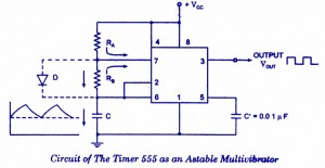
An astable multivibrator, often called a free-running multivibrator, is a rectangular-wave generating circuit. Unlike the monostable multivibrator, this circuit does not require any external trigger to change the state of the output, hence the name free-running. Before going to make the circuit, make sure your 555 IC is working. For that go through the article: How to test a 555 IC for working An astable multivibrator can be produced by adding resistors and a capacitor to the basic timer IC, as illustrated in figure. The timing during which the output is either high or low is determined by the externally connected two resistors and a capacitor. The details of the astable multivibrator circuit are given below.
Take a look @ 555 Ic Pin configuration and 555 block diagram before reading further.
Pin 1 is grounded; pins 4 and 8 are shorted and then tied to supply +Vcc, output (VOUT is taken form pin 3; pin 2 and 6 are shorted and the connected to ground through capacitor C, pin 7 is connected to supply + VCC through a resistor RA; and between pin 6 and 7 a resistor RB is connected. At pin 5 either a bypass capacitor of 0.01 F is connected or modulation input is applied.
Astable Multivibrator Operation
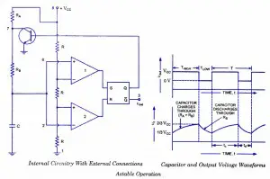
For explaining the operation of the timer 555 as an astable multivibrator, necessary internal circuitry with external connections are shown in figure.
In figure, when Q is low or output VOUT is high, the discharging transistor is cut-off and the capacitor C begins charging toward VCC through resistances RA and RB. Because of this, the charging time constant is (RA + RB) C. Eventually, the threshold voltage exceeds +2/3 VCC, the comparator 1 has a high output and triggers the flip-flop so that its Q is high and the timer output is low. With Q high, the discharge transistor saturates and pin 7 grounds so that the capacitor C discharges through resistance RB with a discharging time constant RB C. With the discharging of capacitor, trigger voltage at inverting input of comparator 2 decreases. When it drops below 1/3VCC, the output of comparator 2 goes high and this reset the flip-flop so that Q is low and the timer output is high. This proves the auto-transition in output from low to high and then to low as, illustrated in fig ures. Thus the cycle repeats.
Astable Multivibrator using 555 IC -Design method
The time during which the capacitor C charges from 1/3 VCC to 2/3 VCC is equal to the time the output is high and is given as tc or THIGH = 0.693 (RA + RB) C, which is proved below.
Voltage across the capacitor at any instant during charging period is given as,vc=VCC(1-et/RC)
The time taken by the capacitor to charge from 0 to +1/3 VCC
1/3 VCC = VCC (1-et/RC)
The time taken by the capacitor to charge from 0 to +2/3 VCC
or t2 = RC loge 3 = 1.0986 RC
So the time taken by the capacitor to charge from +1/3 VCC to +2/3 VCC
tc = (t2 – t1) = (10986 – 0.405) RC = 0.693 RC
Substituting R = (RA + RB) in above equation we have
THIGH = tc = 0.693 (RA + RB) C
where RA and RB are in ohms and C is in farads.
The time during which the capacitor discharges from +2/3 VCC to +1/3 VCC is equal to
the time the output is low and is given as
td or TL0W = 0.693 RB C where RB is in ohms and C is in farads The above equation is worked out as follows: Voltage across the capacitor at any instant during discharging period is given as
vc = 2/3 VCC e- td/ RBC
Substituting vc = 1/3 VCC and t = td in above equation we have
+1/3 VCC = +2/3 VCC e- td/ RBC
Or td = 0.693 RBC
Overall period of oscillations, T = THIGH + TLOW = 0.693 (RA+ 2RB) C , The frequency of oscillations being the reciprocal of the overall period of oscillations T is given as
f = 1/T = 1.44/ (RA+ 2RB)C
Equation indicates that the frequency of oscillation / is independent of the collector supply voltage +VCC.
Often the term duty cycle is used in conjunction with the astable multivibrator.
The duty cycle, the ratio of the time tc during which the output is high to the total time period T is given as
% duty cycle, D = tc / T * 100 = (RA + RB) / (RA + 2RB) * 100
From the above equation it is obvious that square wave (50 % duty cycle) output can not be obtained unless RA is made zero. However, there is a danger in shorting resistance RA to zero. With RA = 0 ohm, terminal 7 is directly connected to + VCC. During the discharging of capacitor through RB and transistor, an extra current will be supplied to the transistor from VCC through a short between pin 7 and +VCC. It may damage the transistor and hence the timer.
However, a symmetrical square wave can be obtained if a diode is connected across resistor RB, as illustrated in dotted lines in figure. The capacitor C charges through RA and diode D to approximately + 2/3VCC and discharges through resistor RB and terminal 7 (transistor) until the capacitor voltage drops to 1/3 VCC. Then the cycle is repeated. To obtain a square wave output, RA must be a combination of a fixed resistor R and a pot, so that the pot can be adjusted to give the exact square wave.
Although the timer 555 has been used in a wide variety of often unique applications it is very hard on its power supply lines, requiring quite a bit of current, and injecting many noise transients. This noise will often be coupled into adjacent ICs falsely triggering them. The 7555 is a CMOS version of the 555. Its quiescent current requirements are considerably lower than that of 555, and the 7555 does not contaminate the power supply lines. It is pin compatible with the 555. So this CMOS version of the 555 should be the first choice when a 555 timer IC is to be used.
Read more: http://www.circuitstoday.com/555-timer-as-an-astable-multivibrator#ixzz0pmSn5C7H
Under Creative Commons License: Attribution


0 komentar:
Posting Komentar